Introduction
The Xilinx marketing department claims that programming of the flash chips of the Virtex 5 is “simple and easy”. While it may be easy once the correct steps have been found, it can be quite difficult to determine what the correct steps are.
This article is a summary of the steps that have been found to work with a Xilinx Virtex 5 (ML506). Solutions have been found for programming all three of the flash types: Platform Flash XL, SPI Flash, and BPI Flash.
It is assumed that the reader already has a familiarity with using the iMPACT program and the dialogs it presents. Being able to program a board without using the flash chips should be sufficient.
Requirements
Xilinx Virtex 5 (ML506)
Xilinx Platform Cable USB II (DLC10)
Xilinx ISE 13.3
SW3 settings
Several bits of switch 3 (SW3) must be set correctly otherwise flash programming will not work. Switch 6 (SW6), located on the back, is unimportant. And switch 8 (SW8), for the GPIO inputs, is unimportant as well.
The following is a description of the meaning of the SW3 settings. Refer to page 35 of ug347 for further information.
      SW3
1 2 3 4 5 6 7 8
---------------
A A A M M M X C
A[1:3] are the address bits. If revisioning is used they can be
used to select which revision. For the simple examples here, it
can be left at zero.
Note: the address bits are actually reversed.
An address of 1 would be A[1:3] = 001.
M[4:6] are the mode bits. These select which flash chip to program
(e.g. Platform Flash, BPI, SPI, etc).
X is not used.
C is the System ACE configuration. Usually this makes no difference
because the CF card is removed. If the card was inserted it would
try to load from there first. It is easiest just to remove the card
and ignore this bit.
The convention used in this document is that a 1 refers to the switch being set or on.
SPI Flash
To program the SPI flash on the Virtex 5 (ML506) SW3 must be set to the following values. Recall from the previous discussion that bits 4, 5 and 6 are the most important to get right.
      SW3
1 2 3 4 5 6 7 8
---------------
0 0 0 0 0 1 0 1
It is assumed that a .bit file has already been created. How to use and configure iMPACT is the primary goal of this document, not how to generate bitfiles with ISE.
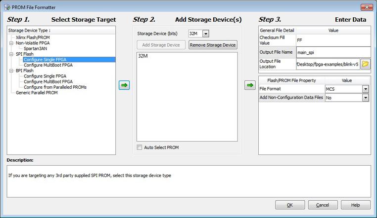
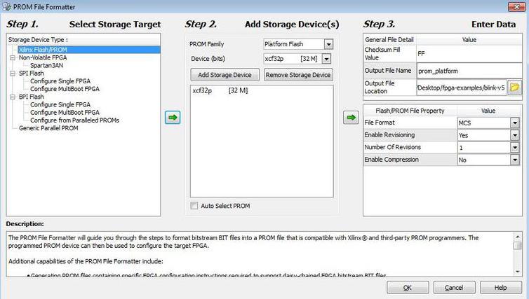
The first step with iMPACT is to create a PROM file. The screen shot below shows the settings that were used.
Notice that the 32Mb (bits) chip was used. This is because the flash chip on the Virtex 5 is the M25P32. Be sure to keep track of the bits and bytes, the Xilinx documentation often switches back and forth between these two unit types.
The PROM file generated will have .mcs extension and will be used in the next step to program the flash.
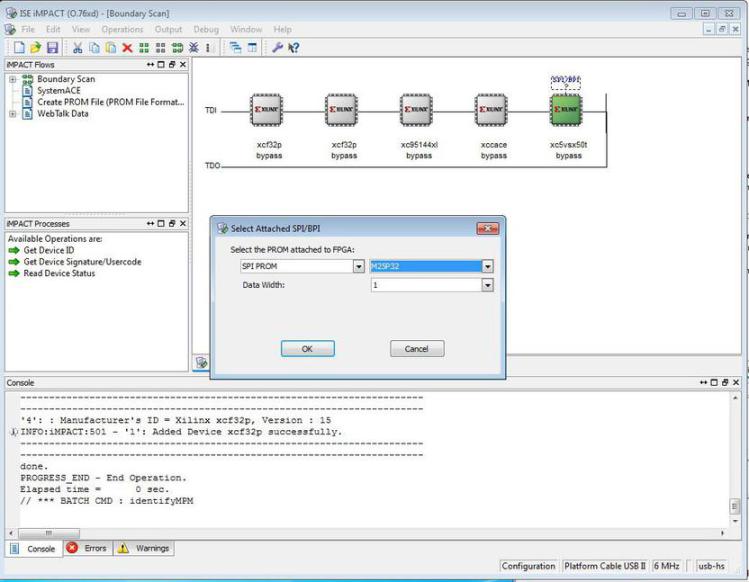
The screen shot below shows the flash programming dialog in iMPACT. When changing from creating a PROM file to programming flash it is recommended to close iMPACT completely and create a new project in each case. In the authors experience this has resulted in the fewest problems.
Notice that in the dialog the M25P32 chip is selected. During PROM generation this label was not available and it was necessary to select 32Mb.
Once the chip is configured the flash can be programmed. It may take 10 minutes or so to burn the chip and it should display a progress bar while it is working.
Once the flash has been programmed the ‘Prog’ button can be pressed to run the program. Or if the board is power cycled it should run the program on startup.
At first it may appear that the program does not run. But in fact it can take 10 seconds or more for the program to start from SPI flash.
BPI Flash
To program the BPI flash on the Virtex 5 (ML506) SW3 must be set to the following values. Notice that only the mode bits have changed compared to programming SPI flash.
      SW3
1 2 3 4 5 6 7 8
---------------
0 0 0 0 1 0 0 1
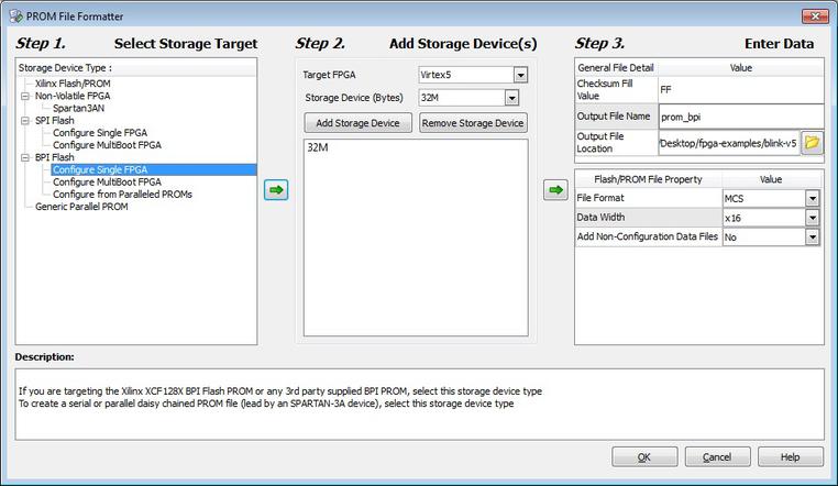
The screen shot below shows the important iMPACT settings during the PROM creation dialog.
Notice that the chip size has been specified as 32MB (bytes). Recall that for SPI flash this same exact dialog used bits instead of bytes. 32MB (bytes) was chosen because the chip used for the BPI flash is the JS28F256P30. This chip can be found on the top of the Virtex 5 board near the north and west buttons.
It may seem that these settings can’t be correct if the chip size is 256Mb (bits) and the PROM dialog specifies 32MB (bytes). But in fact they are identical. Recall that 1 byte equals 8 bits. 256 / 8 = 32. Granted, if the goal was to make these chips as difficult as possible for the end user to configure correctly, this is how it should be done.
Also notice that the data width is set to x16. By default it will be set to x8 and this will not work.
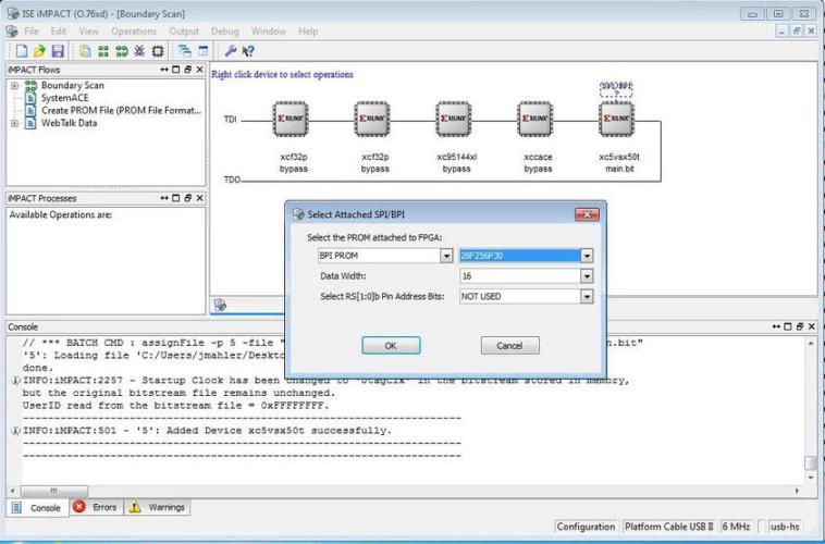
The screen shot below shows the settings during the iMPACT programming
dialog. Notice that the 28F256P30 chip has been chosen.
The numbering in this case omits the JS prefix that would be found
on the actual chip. Also notice that the data width is set to 16.
And the following screen shot shows another dialog during flash programming, the defaults are usually correct in this case.
Once the BPI flash has been programmed the program should run after pressing ‘Prog’ or power cycling the FPGA. It should take less than a second to start running.
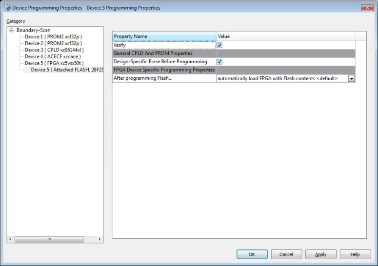
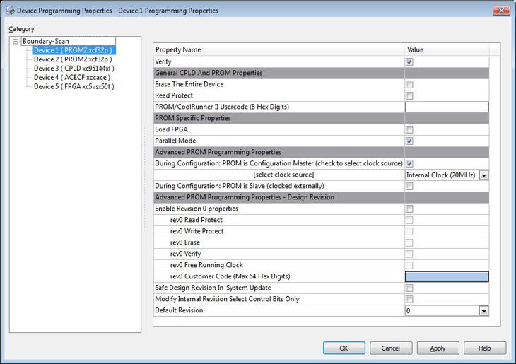
Platform Flash XL
To program the Platform Flash on the Virtex 5 (ML506) SW3 must be set to the following values. Notice that only the mode bits have changed compared to previous configurations.
      SW3
1 2 3 4 5 6 7 8
---------------
0 0 0 1 1 0 0 1
The screen shot below shows the important iMPACT settings during the PROM creation dialog.
Notice that the chip size has been specified as 32Mb (bits) which
corresponds to the xcf32p chip which is being used. Two of these
chips can be found on the board with one on the top and the other on
the bottom.
The screen shot below shows the important iMPACT settings during the flash programming dialog. There are two settings that must be set correctly otherwise the program won’t run and there will be no indication of any error. Parallel Mode must be checked. And the internal clock must be set to 20 MHz.
As usual, once the flash has been programmed the ‘Prog’ button can be pressed or the board can be power cycled to start it running. It should take less than a second to start running.